咨询热线:0769-8991 7065
咨询热线:0769-8991 7065


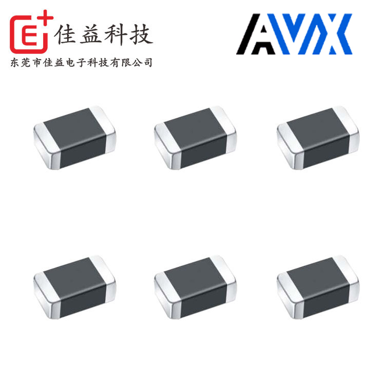
东莞市佳益电子科技有限公司座落于全球著名的制造业基地---东莞市塘厦镇,交通运输方便灵活。凭借良好的企业发展理念和专业技术水平,在电子元件领域迅速崛起。公司走多元化发展道路,现拥有多家生产企业及销售公司。形成了一个覆盖广、稳定、高效的专业销售网络。同时为了扩大产品市场及方便客户采购,本公司设立了5000平方米的物流仓储基地,月库存约50亿支的个品牌元器件,通过现代化的物流操作模式从仓储物流中心转送到全国各地客户手中。
本公司的宗旨:科技创新,精益求精,开拓进取,务实高效。公司经营理念:以人为本,诚信务实,互惠互利。公司服务宗旨:“一流的技术,一流产品、周到的客户服务”是我们的宗旨。“客户满意”是我们永恒的追求。

性能 Characteristics 佳益科技
The device must be quite thick(high profile)since thelines of flux are parallel to its axis(i.e.inductor crosssection is width x thickness)and therefore,a thin partcannot be efficiently designed.Such high profile devicesmay actually skid across the board during high speedpick-and-place assembly.End terminations of the partare only partial.Furthermore,the wire conductor isdelicate,particularly at its point of contact with thetermination,leading to reliability concerns.
A New Design for SMD Inductors
An alternative approach which provides for a highfrequency inductor that is both small and rugged is toconstruct the device from layers on a substrate.Thisapproach,a common method of forming inductors onhybrids and which is also utilized in various wire bond-able inductor chips,has now been incorporated into atrue SMD device.
Figure 1 depicts the structure of the ACCU-L induc-tor.Multiple inductor layers are constructed on a non-magnetic substrate of alumina.Each layer consists of aconductor spiral which is coated with an insulatinglayer.The insulator includes a via connect to the over-laying spiral.The uppermost layer seals the device.Thetotal thickness of these layers is typically less than0.3mm and the device thickness(substrate plus inductorlayers)is only 0.9mm.
The manufacturing method used in building thisinductor is photolithography.This technique,which hasbeen extensively developed in the microelectronicsindustry,allows simultaneous formation of thousands ofdevices on a single substrate.The individual devicesmay then be separated from each other upon completionof all layers.
Bare inductor chips would,of course,be incompatiblewith surface mount assembly techniques.Figure 1shows that this inductor includes full end terminationwith lands.These terminations are formed of soldercoated nickel plate.It is this termination which convertsthe inductor chip into a true SMD inductor.
Summary
The ACCU-L SMD inductor meets both present andfuture needs of high frequency applications.It is small,rugged,includes full end terminations and exhibitsexcellent electrical performance.The multilayer con-struction provides a high level of control on the electri-cal and physical characteristics of the inductor,givingconsistent characteristics within a lot and on a lot-to-lotbasis.The ACCU-L inductor fills a void created by theinability of earlier technologies to satisfy continuingminiaturization and manufacturability requirements ofhigh frequency circuits.
SMD Inductor Guide
A Glossary of Important Inductor Parameters forHigh Frequency Applications
Inductance.High inductance values are not a factorin most high frequency applications.1.8nH to 39nH istypically the range of interest.The critical factors arethe stability and tolerance of the inductance at operat-ing frequency.Note that accurate measurement of theselow values is not trivial.Even at low frequencies(~10MHz),instruments available today exhibit measure-ment accuracy of no better than about±5%for an induc-tance of 10nH.At typical application frequencies(≥450MHz),measurement accuracy may be even furtherdegraded by parasitic capacitance of inadequately char-acterized test fixtures.
Parasitic Capacitance.All inductors include a certaincapacitance characteristic.This capacitance is derivedfrom the mutual proximity of the coil windings.Thecapacitance is further magnified by the inductor struc-tural materials,especially if these are of high dielectricconstant.It is critical for high frequency inductors thatthe parasitic capacitance be minimized since it deter-mines the device SRF.
SRF.Self resonant frequency of the inductor is thatfrequency at which parallel resonance is achievedbetween the device inductance and parasitic capaci-tance.Inductor Q drops to zero at SRF.It is quiteimportant,therefore,that inductor SRF be much higherthan the application frequency.
Resistance.In addition to inductance and parasiticcapacitance,the inductor also exhibits resistance.At lowfrequencies,the resistance of the conductor track is thedetermining factor in inductor Q.At very high frequen-cies,the resistivity of the conductor material is moreimportant than the resistance.(resistance=resistivity xconductor length)cross sectionThis is due to the skin effect whereby high frequencycurrent flow is largely restricted to the surface layer ofthe conductor.For high Q at high frequency,it is there-fore important that the coil conductor be constructed ofa metal with low resistivity.


手 机:13929253003 王小姐
Q Q:2365818764
电 话:0769-89917065
传 真:0769-82616686
办公地址:东莞市塘厦大道北552号3H创客中心312
电子邮箱:goodonecn@163.com
上一篇:已经没有了