咨询热线:0769-8991 7065


主要销售产品:贴片电容,贴片电阻,钽电容,贴片电感磁珠等系列产品。销售的产品线渗透到各个电子行业:手机、电源、小家电、液晶电视、显示器、机顶盒、便携式电子设备等。
公司拥有先进的生产设备和雄厚的技术力量,设有一流的产品研发中心和检测中心,严格按照IS09000-2000质量认证、ISO14000环境认证体系进行管理,把“质量、诚信”作为公司长久发展的基础,并将这一信念传输给每一位职员。
我们坚持“以客为主,以人为本”的经营理念,秉承优良品质与完美服务的一贯宗旨,以客户的利益为出发点,提供快捷、高质、高效的专业服务。

应用 Applications 佳益科技
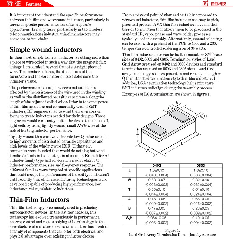
Thin-film technology allows for the deposition of low ESRline width structures to the micron and below level.Theresult of such small structures yields extremely tighttolerance inductors in virtually any value imaginable.Typically,inductor tolerances as tight as 0.05 nH areavailable in low value 0402 and 0603 case sizes.The 0805case size is available in values as low as 1.2nH andtolerances as tight as 0.1nH.
Though the maximum value of thin-film inductors is lessthan air-wound inductors’maximum values of 6.8nH and22nH are available in 0402 and 0603/0805 sizes respectively.As RF frequencies increase,lower-value inductors becomethe more necessary in circuit design.The tight tolerance and electrical characteristics of thin-film inductors is stable pre-and post-processing and haveoutstanding stability in application.Sometimes theprocessing of wirewound devices can interfere with theirspecific inductance values and make adjustmentsnecessary.Further,the low height of thin-film devicesmakes them able to withstand high G forces and vibrationwhile maintaining a high degree of electrical stability.Thin-film inductors are also highly stable in environmentalextremes of temperature,humidity,moisture and time.
Thin-Film InductorApplication Advantages
Thin-film inductors offer significant advantages overwirewounds for an ever-increasing number of applications(even though wirewound inductors may have a larger valuerange,or a higher Q and even a higher current capacity).Infact the standard terminated thin-film device can have acurrent capability of 1000mA.Depending on application,the thin-film inductors’lower Q is an actual advantage.Oneexample of this is in frequency compensation on broadbandamplifiers.Previously a resistor/inductor combination wasused.A thin-film inductor has the capability of replacingthose two components with a single component solution.Thus improving system reliability while saving circuit sizeand weight.
Thin-film inductors’maximum value is less than that ofwirewounds’inductance values.However wirewounds maynot be available in low inductance values and this isanother problem.At some point,when designing a circuit(like a multi-GHz oscillator,for example)it is just notpossible to obtain an extremely low value wirewoundinductor.Manufacturing techniques do not exist to buildsuch a low value wirewound part in a cost-effectivemanner.
At that point,the designer is left with the choice ofcreating a low value inductor with a meandering PC boardtrace design or choosing a thin-film inductor chip.In thiscase though the PC Board trace inductor could beconsidered free,it consumes a lot of board space and willhave many disadvantages such as having parasitic effectsassociated with it.One interesting case study even showedthe cost of the PCB actually increasing due to the finewidth demands of the printed inductor.In many cases it ismuch more efficient to choose the thin-film inductor.
It is also important to note that thin-film inductors offerdesigners a miniature intermediate-to-high Q inductor thatis electrically repeatable on a lot-to-lot basis and,mostimportantly,thin-film inductors offer extremely tighttolerance options for designers.This is significant andsolves many problems for designers.
Thin-film inductors usage is dramatically increasing due tofrequency spectrum crowding,narrow band circuit needsand maximum useable frequency band increases.Further,significant progress is being made with increasing the Qfactor and maximum value range of the part,making itmore and more often the necessary solution for designengineers in the wireless field.


手 机:13929253003 王小姐
Q Q:2365818764
电 话:0769-89917065
传 真:0769-82616686
办公地址:东莞市塘厦大道北552号3H创客中心312
电子邮箱:goodonecn@163.com
上一篇:AVX帖片电感_AVX贴片功率电感_AVXSMD贴片电感_AVX电感全系列
下一篇:已经没有了